The semiconductor industry depends on precision, reliability, and secure transportation at every stage of the supply chain. As semiconductor components become smaller, more advanced, and increasingly sensitive, manufacturers face growing challenges in protecting products during storage and shipping. This is where effective semiconductor packaging solutions become essential.
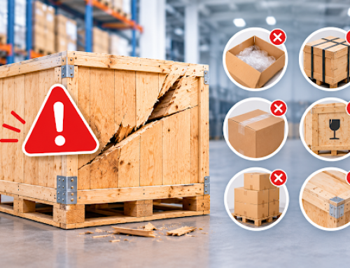
From fragile semiconductor wafers to finished electronic components, improper packaging can lead to contamination, physical damage, moisture exposure, and costly production delays. Companies require specialized packaging systems, including custom pallets and crates, skid and pallet solutions, and advanced protection methods designed specifically for semiconductor applications.
Common Packaging Challenges in the Semiconductor Industry
1. Protecting Sensitive Semiconductor Components
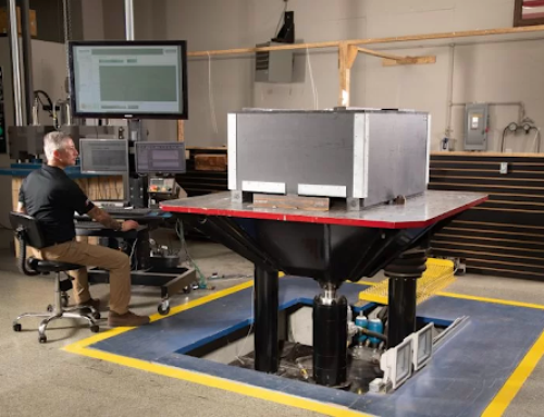
Semiconductor products are highly vulnerable to vibration, shock, electrostatic discharge (ESD), and environmental changes. Even minor damage during transportation can affect product performance and create significant financial losses.
Traditional packaging methods often fail to provide the level of protection required for modern semiconductor devices. Manufacturers need engineered packaging solutions that control movement, reduce impact, and maintain product integrity throughout the supply chain.
2. Managing Complex Semiconductor Packaging Requirements
The semiconductor packaging process involves multiple stages, including assembly, testing, inspection, and transportation. Each stage requires packaging that meets strict industry standards.
Challenges include:
- Maintaining cleanroom compatibility
- Preventing contamination
- Protecting against moisture and temperature changes
- Ensuring safe handling during logistics
- Reducing packaging waste while maintaining durability
A customized approach helps semiconductor manufacturers overcome these challenges by creating packaging systems designed around specific product dimensions and handling requirements.
How Custom Pallets and Crates Improve Semiconductor Packaging
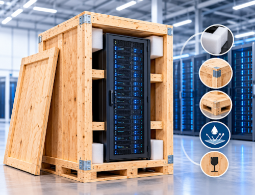
Standard shipping solutions are often not suitable for sensitive semiconductor equipment and components. Custom pallets and crates provide a stronger and more reliable option by being designed specifically for the product being transported.
Benefits include:
- Improved structural support during transportation
- Better protection against impact and vibration
- Optimized space utilization
- Reduced risk of product damage
- Easier handling during loading and unloading
Custom-designed packaging also helps manufacturers meet international shipping requirements while maintaining product safety across long-distance transportation routes.
Advancements in Semiconductor Packaging Technology
Modern semiconductor packaging technology continues to evolve as manufacturers develop smaller and more powerful electronic devices. Advanced packaging methods require equally advanced transportation and protection solutions.
Some key trends include:
- Lightweight but stronger packaging materials
- Reusable packaging systems
- Smart tracking solutions
- Sustainable packaging designs
- Precision-engineered protective structures
Companies that invest in advanced packaging solutions can improve supply chain reliability while reducing damage-related costs.
Choosing the Right Semiconductor Packaging Partner
Selecting an experienced packaging provider is critical for semiconductor manufacturers. The right partner understands the unique requirements of semiconductor logistics and can develop solutions based on product size, weight, transportation method, and environmental conditions.
A specialized packaging company can provide:
- Custom engineering and design support
- Durable pallets, crates, and skids
- Industry-specific protection solutions
- Packaging optimization for cost and performance
For businesses looking for reliable semiconductor packaging solutions, working with an experienced provider helps ensure products arrive safely and efficiently.
Conclusion
The semiconductor industry faces complex packaging challenges due to sensitive components, strict quality requirements, and demanding global supply chains. Investing in customized solutions such as custom pallets and crates, engineered skid and pallet systems, and modern semiconductor packaging technology helps companies reduce risks and improve transportation efficiency.
With the right packaging strategy, semiconductor manufacturers can protect valuable products, minimize delays, and build a more reliable supply chain.
FAQs
1. What is semiconductor packaging?
Semiconductor packaging is the process of protecting and preparing semiconductor components for handling, testing, storage, and transportation while maintaining product reliability.
2. Why are custom pallets and crates important for semiconductor packaging?
Custom pallets and crates provide specialized protection against vibration, impact, and environmental risks that standard packaging cannot handle.
3. How does the semiconductor packaging process work?
The semiconductor packaging process includes assembly, protection, testing, inspection, and preparation of semiconductor devices for final use or transportation.
4. How does advanced semiconductor packaging technology improve supply chains?
Modern semiconductor packaging technology improves product protection, reduces transportation damage, supports sustainability, and increases supply chain efficiency.